


Insulator Semiconductor Multilayer Structures for Nanoelectronic Devices
Joachim Wollschläger, Karl Hofmann, Marcus Bäumer
The extremely restricted size of structures used for nanoelectronic devices induce new physical properties which are governed by quantum physics. For instance, the tunnelling effect drives resonant tunnelling devices. Keypoints to the functionality of these tunnelling devices are insulator and semiconductor films which both have only nanometer thickness. These insulator semiconductor multilayer structures can only be produced with high quality if lattice matched materials are used. Here the combination of CaF2 and Si is outstanding due to the very small lattice mismatch of only 0.5%. In addition, these structures are compatible to the well established Si technology. In the meantime it has been demonstrated that resonant tunnelling diodes, which are based on CaF2/Si structures, excellently perform [1] Nevertheless this material system is still under investigation due to its unique properties. On the one hand, the growth of CaF2 on Si(111) is well established [2]. These films grow layer-by-layer since CaF2 wets Si due to the advantageous relation between surface energies and interface energy. On the other hand, problems appear for the inverse system Si/CaF2 due to the inverted relation of surface energies. Attempting to improve the film quality by solid phase epitaxy (SPE) fails since semiconductor films dewet at lower temperatures than necessary to recrystallize these films [3]. Therefore special techniques as surfactant-mediated SPE have been developed to produce homogeneous ultrathin Si films on CaF2 films [4]. If surfactants are not used during the annealing of room temperature deposited semiconductor films the dewetting of the semiconductor films starts at lower temperatures than necessary to recrystallize Si films [4]. This property is attributed to the decrease of surface energy of the semiconductor film due to surfactants. We studied the structure, morphology, and stoichiometry of Si/CaF2/Si(111) and Ge/CaF2/Si(111) by means of Grazing Incidence X-Ray Diffraction (experiments performed at HASYLAB (DESY)), Spot Profile Analysis of Low Energy Electron Diffraction (SPA-LEED) and X-Ray Photoelectron Spectroscopy (XPS).
[1] C.R. Wang, M. Bierkandt, S. Parotta, T. Wietler, and K.R. Hofmann, Appl, Phys. Lett. 86 (2005) 033111
[2] J. Wollschläger, in: Recent Research Developments in Applied Physics, Vol. 5-II, ed. S.G. Pandalai (Transworld Research Network, Trivandrum, India, 2002) pp. 621-695.
[3] J. Wollschläger, E. P. Rugeramigabo, and C. Deiter, Surf. Sci., accepted
[4] J. Wollschläger, C. Deiter, M. Bierkandt, A. Gerdes, M. Bäumer, C.R. Wang, B.H. Müller, and K.R. Hofmann, Surf. Sci. 600 (2006) 3637
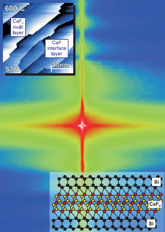
Figure below:
Reciprocal space mapping of Si/CaF2/Si multilayer structure recorded by synchrotron radiation. The well developed intensity oscillations demonstrate the high quality of the multilayer structure. Experiments are performed at HASYLAB (DESY, Hamburg, Germany).
Upper inset: STM micrograph of two monolayer of CaF2 deposited on Si(111). While the interface layer shows residual point defects the additional film is extremely smooth.
Lower inset: Model of Si/CaF2/Si multilayer.