


Nano Center South (NanoSYD)
The Nano Center South (NanoSYD) (www.nanosyd.sdu.dk) has been founded beginning of 2007 at the new premises of the University of Southern Denmark (SDU) in Sønderborg at the German/Danish border. NanoSYD concentrates the nanotechnological activities at SDU, focusing on nanophotonics, nano- and microstructure formation, nano-integration, organic electronics and photonics, mathematical modeling as well as laser materials treatment. NanoSYD collaborates strongly with the main campus of SDU in Odense,and here within the Faculty of Engineering with the SENSE institute for sensor technology and within the Faculty of Natural Sciences with nanobiological related activities among others concentrating on nanobiosensors, membrane physics, proteomics etc. NanoSYD is also housing a Graduate School on mesoscopic structures, dynamics and optics (www.meso.sdu.dk) and diverse techtrans activities such as the start up company Nanofiber A/S (www.nanofiber.dk). Head of NanoSYD is Professor Horst-Günter Rubahn.
NanoSYD is equipped with a cleanroom facility that houses on an area of more than 100 squaremeters state-of-the-art class 100 cleanroom technology for educational, research and small-scale process purposes. The cleanroom is linked to the Mads Clausen Institute for Product Innovation and it joins both from its location and its intentions university and industry needs. The university uses the cleanroom also for student and researcher instructions to modern semiconductor micro- and nanotechnology.
The cleanroom at NanoSYD allows semiconductor production via photolithography, dry and wet etching processes etc., but is by no means limited to that. Processing and characterization biocompatible or catalytic active surfaces is also possible. Ultrathin films of conducting, semiconducting and insulating materials can be grown and structured on a micron-scale (conventional photolithography), submicron-scale (excimer laser etching) and nanoscale (electron-beam lithography). Morphological characterization also can occur on a large scale (epifluorescence, dark field and interference microscopy) and on a nanometric scale (atomic force microscopy, scanning electron microscopy). NanoSYD houses in fact a new field emission scanning electron microscope with a resolution on the nanometer size scale at voltages of not more than 1kV this allows researchers to investigate with very high resolution also fragile dielectric and organic thin films or structures.
Some exemplary initial projects for the cleanroom include the generation of artificial membranes, nanofiber integration, SERS substrates for bacteria sensing, testing and device implementing of nano- and mesoporous materials, rapid prototyping of microstructured fluidic elements and printed self-assembled monolayers,. This research bridges basic nanoscience and applied nano- and microtechnology. NanoSYD is strongly affiliated with DANFOSS on the one-hand-side and the university nanotechnology and mechatronic laboratories in Sønderborg as well as the Center for Product Development (CPD) on the other hand. The university laboratories add modern surface characterization and laser techniques including advanced laser materials processing to the portfolio of the cleanroom.
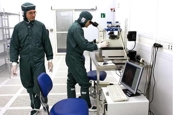
Professor Rubahn (left) in the clean room facility of NanoSyd